
In brief
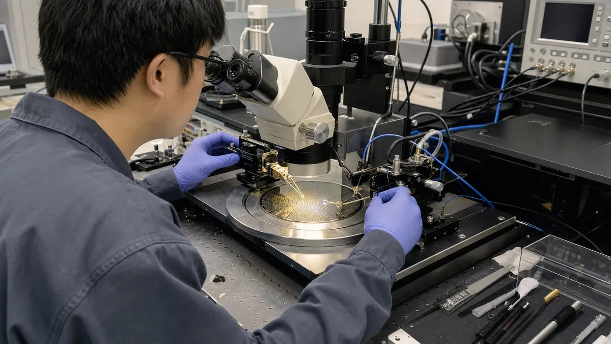
Choose a manual probe station by validating the complete measurement chain, not wafer diameter alone. Wafer and pad geometry, probe arms, microscope, chuck, RF or DC cabling, environment, calibration, instruments, operator procedure, and data records must together support repeatable probe landing and measurement.
Key takeaways
- Document wafer or substrate geometry, pad pitch, probe count, travel, microscope access, and contact constraints before selecting the station.
- Specify RF calibration and cable routing or DC guarding, leakage, light, grounding, and environmental controls according to the measurement type.
- Acceptance should prove repeatable landing, path integrity, connected-instrument behaviour, and traceable data with representative devices or references.
A manual probe station is a positioning and contacting platform inside a larger measurement system. It does not create traceability, low leakage, calibrated S-parameters, or repeatable device parameters by itself. Those outcomes depend on the DUT geometry, probe and contact mechanics, chuck and microscope, cabling, instrument configuration, environmental control, calibration method, operator procedure, and uncertainty evaluation.
Define the measurand before selecting hardware
Start by naming the quantity being measured and the decision it supports. Examples include DC leakage at a stated bias and temperature, an I-V curve with a defined sweep rate, capacitance at a stated frequency and AC level, two-port S-parameters at a defined on-wafer reference plane, or sheet resistance using a specified geometry. “Wafer probing” is not a measurement method.
For every test, record the stimulus, expected response, source and measurement ranges, compliance or protection limits, settling rule, environmental condition, contact configuration, data reduction, and acceptance limit. Then identify whether the result is for exploratory characterization, process monitoring, device screening, design verification, or a formal conformance decision. The required evidence and uncertainty are different.
Freeze wafer, die, pad, and contact geometry
The station-selection package should include wafer diameter and thickness, backside condition, die map, edge exclusion, substrate or film type, pad size and pitch, passivation opening, pad metallurgy, contact count, probe arrangement, and any keep-out or fragile structures. Full wafers, diced die, coupons, packaged devices, and irregular substrates need different holding and access strategies even when their outer dimensions fit the same chuck.
Contact geometry affects the measurand. In a collinear four-probe sheet-resistance method on an ideal large uniform sheet, a familiar screening relation is R_s = (pi / ln(2)) * (V / I) * F, where F represents the applicable thickness, edge, and geometry corrections. The equation is not a universal conversion for arbitrary wafers. NIST’s certified-resistivity work shows why configuration, spatial characterization, correction factors, and uncertainty must be controlled. The same principle applies more broadly: a probe station must support the selected method, not merely hold the sample.
Define acceptable probe force or overtravel through the probe manufacturer’s method and the pad process window. Do not invent one universal force. Record the landing direction, scrub or skate expectation, maximum mark envelope, tip inspection interval, and replacement trigger. Microscope images can document a mark, but they cannot replace electrical evidence of contact quality.
Separate DC, low-current, C-V, and RF path requirements
A DC path needs voltage/current range, compliance, contact resistance strategy, force/sense topology, grounding, and safe bias removal. Low-current work adds fixture insulation, guarding, triax routing, dark conditions where relevant, humidity control, contamination management, settling time, and an open-path background test. Guarding reduces leakage driven by voltage differences; shielding reduces coupled interference. They solve different problems.
C-V work requires the frequency and AC level, DC bias, cable compensation, contact configuration, parasitic model, and settling rule. A station advertised for I-V and C-V does not prove that a particular cable and chuck configuration meet the required residual capacitance or loss.
An RF path needs probe type and pitch, connector family, cable routing, calibration substrate, calibration algorithm, frequency span, source power, IF bandwidth, and the on-wafer reference plane. NIST’s on-wafer calibration work shows that multiline TRL and calibration-comparison methods address systematic errors that a visually good landing cannot reveal. When a cable or probe arm moves after calibration, define the allowable movement and the verification check.
Integration evidence before quotation
Treat the station, probes, optics, chuck, environment, cables, calibration artefacts, instruments, and software as one measurement chain. The following scope matrix catches the common gaps before a standalone station quotation hides them.
| Integration area | Evidence to provide | Rework trigger |
|---|---|---|
| Device geometry | Wafer or substrate size, die map, pad pitch and metallurgy, probe count, keep-out zones, and representative drawings | Station capacity is discussed without a probe map or DUT geometry |
| RF measurement chain | Probe pitch and type, frequency span, cable path, calibration substrate and plane, VNA ports, connector-care plan, and required result format | S-parameter requirements do not identify the probe, cable, calibration, or connected-instrument configuration |
| DC and leakage chain | SMU range and compliance, guarding, shielding, triax/coax choice, light and contamination control, settling rule, and background check | Low-current repeatability is assigned to the SMU before the environment and interconnect are controlled |
| Operator repeatability | Microscope configuration, chuck movement, landing procedure, training record, and representative load/align/measure workflow | Results depend on one experienced operator and cannot be repeated by the receiving team |
| Data and acceptance | Wafer ID, die coordinates, probe and instrument settings, calibration/verification state, operator, time, raw data, and export format | Hardware is delivered without a reviewable measurement record and release workflow |
Control mechanics, optics, and environment
Mechanical acceptance should measure reach and repeatability, not only quoted travel. Challenge centre and edge die access, platen obstruction, manipulator collisions, cable side-load, chuck flatness, Z clearance, and the operator’s view during landing. For small pads, the microscope must show both the tip and the target with enough depth and illumination control to judge contact without forcing a damaging overtravel.
Vibration, airflow, floor motion, acoustic excitation, thermal drift, light, humidity, and nearby RF or power equipment can change results. Record the station location and the states used during acceptance. A result taken with the enclosure closed and fans off is not directly comparable with production use if the normal workflow opens the enclosure or runs nearby equipment.
For heated or cooled probing, define the actual temperature option, chuck range, sample-temperature measurement, ramp and soak criteria, cable and probe compatibility, condensation or purge controls, and safe-touch/interlock method. Do not infer a temperature range from the base station description unless that configured option is documented.
Calibration, verification, and uncertainty
Calibration establishes a measurement relationship under stated conditions; verification checks whether the system remains fit for use. A practical method can include instrument calibration status, open/short or leakage checks, a known resistor or device, RF calibration standards, and a post-calibration verification artefact. Record failures and prevent data release when a critical verification is outside its limit.
Build an uncertainty or measurement-risk list around the actual measurand. Candidate contributions include instrument calibration and noise, source accuracy, contact repeatability, probe placement, cable movement, reference-standard value, temperature, chuck non-uniformity, leakage background, light sensitivity, humidity, data-fitting method, and operator. Not every contribution is significant for every method. The JCGM GUM provides the framework; it does not supply application-specific values.
Probe-station decision matrix
| Workflow | Hardware and method priorities | Release evidence |
|---|---|---|
| DC I-V | Stable contact, compliance, force/sense routing, safe bias removal, repeatable sweep recipe | Repeated landings, known reference, compliance event, raw curve and setup record |
| Low-current leakage | Guarding, triax path, insulation, dark/shielded enclosure, cleaning and environmental control | Open-path background, short/zero check, reference device, settling record, environmental state |
| C-V | Stable bias, AC frequency/level, parasitic compensation, contact topology | Compensation file, known capacitor/device, repeatability after reload |
| RF S-parameters | Probe pitch, calibration substrate, cable stability, connector care, reference plane | Calibration and verification artefact, before/after reload checks, Touchstone metadata |
| Four-probe or Hall method | Defined geometry, current reversal or method sequence, temperature and spatial plan | Controlled worksheet, geometry corrections, reference material where appropriate |
Acceptance sequence and rejection criteria
- Inspect and identify the chuck, manipulators, probes, cables, adapters, and configured options.
- Demonstrate access to representative centre, mid-radius, and edge sites without collision or cable pull.
- Perform repeated unload, load, align, land, measure, and lift cycles using a defined method.
- Run the electrical zero, open, short, reference, or RF verification relevant to the measurand.
- Challenge one fault: lifted probe, wrong site, compliance, failed calibration, open contact, or operator abort.
- Export the record and confirm it contains wafer ID, die coordinates, station and probe configuration, instrument IDs, calibration/verification state, operator, time, raw data, and result status.
Reject release if the station fits the wafer but cannot reach required sites; if cable force moves a landed RF probe; if low-current background is not small enough for the method; if a verification failure does not block result release; if probe marks exceed the device process limit; or if two operators cannot follow one controlled landing and data procedure.
Illustrative worked example - not a customer case
Assume a hypothetical lab wants to measure a nominal 100 ohm thin-film test structure and a separate low-leakage device. Five unload/reload measurements on the resistor are close, but the leakage result changes whenever room lighting is switched. The station is not accepted for leakage work merely because the resistor is repeatable. The team adds a light-state requirement, checks the open guarded path, records settling time, and repeats the leakage verification with the enclosure in its normal operating state.
For an RF screen, assume the same lab plans a 10 GHz two-port measurement. Calibration succeeds, but the verification device changes after the manipulator cable is repositioned. The team changes strain relief and defines a cable home position before repeating calibration and reload checks. No numerical pass limit is supplied here because that limit must come from the lab’s measurement requirement and uncertainty budget.
This is an invented teaching example. It is not an XGY Tek or customer project, not measured product performance, and not evidence that one station configuration supports both methods.
Source-to-claim map
| Engineering statement in this article | Primary or official basis |
|---|---|
| On-wafer RF accuracy depends on calibration standards, reference plane, and verification | NIST on-wafer calibration programme |
| Wafer-resistivity results require controlled configuration, spatial characterization, and uncertainty | NIST SP 260-131 certification work |
| Geometry, contact layout, temperature, equipment, and operator belong in the method record | NIST resistivity and Hall guidance |
| Precision coaxial connector care and repeatability affect the probe feed path | IEEE 287.3-2021 |
| Semiconductor terminology, ratings, and measurement context are device-method dependent | IEC 60747-1 |
| Measurement uncertainty and metrology terms need explicit definitions | JCGM GUM and VIM |
| Laboratory competence and consistent operation involve more than equipment ownership | ISO/IEC 17025:2017 |
XGY product-data boundary
The XMPS-208 product page lists an 8-inch chuck, 210 mm by 210 mm X/Y travel, less than 2 um probing resolution, microscope lift adjustment precision of 0.5 um or better, and a 400X continuous-zoom APO objective configuration. It also describes DC-to-THz and I-V/C-V/RF readiness plus upgrade paths; these are platform boundaries, not proof of accuracy for every method. The related GPR page lists GS/SG probes from DC to 67 GHz, 50 to 300 um pitch, and connector/model options. Final suitability still requires the configured probe, calibration substrate, instrument, cabling, environment, and acceptance evidence. No unlisted temperature range or system-level fA accuracy is asserted here.
Product fit
Where XGY Tek fits
The listed XMPS-208 manual probe station and GPR-series RF probes can be reviewed as parts of the measurement chain described here. Final suitability depends on wafer and pad geometry, probe configuration, microscope access, RF or DC requirements, environment, calibration, connected instruments, and representative acceptance evidence.
Probe Stations
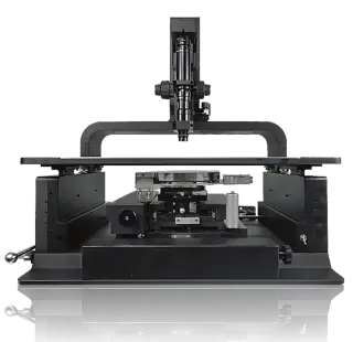
XMPS-208 Manual Probe Station
XGY XMPS-208 is an 8-inch manual probe station for chip-level characterization and IC verification across DC to THz measurements. It combines I-V/C-V/RF test capability, <2 µm probing resolution, 210 mm × 210 mm X/Y travel, an 8-inch multi-hole vacuum chuck, and 400X continuous zoom APO objectives.
View product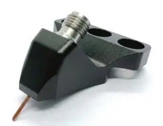
Probe Stations
GPR Series RF Probe
XGY GPR Series is a range of RF probes that use 3D MEMS micromachining and nickel-alloy tips for stable, repeatable on-wafer contact from DC to 67 GHz. GS and SG configurations support 50 to 300 µm pitch options for probe-station measurement setups.
View productFAQ
Frequently asked questions
What makes probe-station selection different from ordinary instrument selection?
The station defines the physical measurement plane. Pad geometry, probe landing, chuck state, microscope access, shielding, cable routing, and the calibration substrate can change the result as much as the connected SMU or VNA, so the station and instrument chain must be scoped together.
Is wafer diameter enough to choose a manual probe station?
No. Wafer diameter only confirms one mechanical boundary. The buyer also needs pad pitch, probe count, chuck travel, microscope field of view, probe-arm stability, cable routing, shielding, thermal requirement, and operator access. A station that holds the wafer can still fail the measurement method.
What should be checked for RF probing?
Check probe type, pitch, frequency range, calibration substrate, cable bend radius, probe-arm stability, connector torque practice, and whether the calibration plane survives probe landing and fixture movement. RF probing should be reviewed as a signal-chain problem, not only a microscope problem.
What makes low-current wafer probing difficult?
Low-current measurements can be limited by fixture leakage, humidity, cable insulation, light, grounding, contamination, and unguarded connections. If leakage is in the picoamp or lower range, the quote should include guarding, shielded enclosure, triax or low-leakage cabling, cleaning practice, and environmental expectations.
What should acceptance prove before the station is released?
Acceptance should prove stable contact, microscope usability, probe landing repeatability, calibration or zero-check workflow, connected instrument behavior, data export, and operator procedure. For RF or leakage work, a known reference path or device is more useful than a generic visual inspection.
Keep exploring
Related technical resources
Related articles
Procurement Checklist
Semiconductor Test Fixture Validation Checklist
A semiconductor test fixture validation checklist covering probe access, SMU paths, RF cables, thermal conditions, repeatability, reports, and acceptance evidence.
Read article
Technical Article
Source Measure Unit Selection for Semiconductor Test
A practical guide to selecting source measure units for semiconductor characterization, wafer probing, production validation, and automated test.
Read article
Technical Article
Phase-Stable RF Test Cable Buying Guide
How to evaluate phase-stable RF test cables for VNA measurement, production test, field use, and mmWave benches.
Read article