
Products
Probe Stations
Probe Stations and RF Probes for Semiconductor Wafer Test
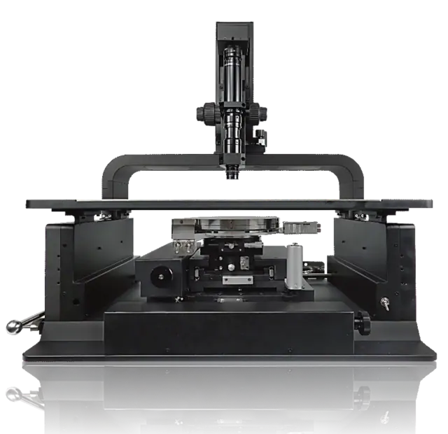
XGY Tek supplies manual probe stations and RF probes used in semiconductor fabs, university cleanrooms, and failure-analysis labs. Configurations support wafers up to 8 inches on a multi-hole vacuum chuck, with manual XYZ staging over 210 mm x 210 mm, probing resolution under 2 um, and upgrade paths for high- and low-temperature aging environments.
The station should be scoped from the DUT and measurement path: wafer size, die pad pitch, DC or RF probe type, probe pitch, high-voltage or low-current need, triax or coax cabling, chuck temperature, microscope plan, vibration sensitivity, shielding, and exported data workflow.
For station and RF probe planning, see our probe station selection guide. Safety, particle monitoring, and calibration documentation requirements are confirmed during quotation.
Probe Stations product list
Best fit
Chip-level characterization and IC verification using manual wafer probing.
XMPS-208 Manual Probe Station
- Chuck size: 8 inch (200 mm)
- Probing resolution: < 2 µm
- Frequency domain capability: DC to THz measurements (Measurement)
- Supported tests: I-V / C-V / RF (Measurement)
Best fit
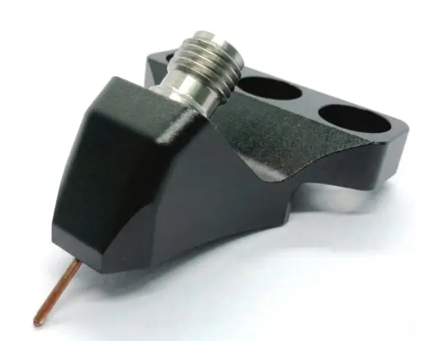
Repeatable on-wafer RF contact for probe-station S-parameter measurement.
GPR Series RF Probe
- Frequency range: DC to 26 / 40 / 50 / 67 GHz
- Configuration: GS, SG
- Pitch: 50 to 300 µm
- Impedance: 50 Ω
Selection path
Probe-station selection path
Choose the station around wafer handling and measurement access, then match the RF probe to frequency, contact geometry, and pitch.
- XMPS-2088-inch manual probe station
- Coverage
- 8-inch wafer; manual XYZ; DC to THz I-V / C-V / RF; < 2 µm probing resolution
- Best fit
- Chip-level characterization and IC verification using manual wafer probing.
- GPR SeriesGS / SG RF probe
- Coverage
- DC to 26 / 40 / 50 / 67 GHz; 50 to 300 µm pitch; 50 Ω impedance
- Best fit
- Repeatable on-wafer RF contact for probe-station S-parameter measurement.
Frequently Asked Questions
What wafer sizes and applications does the XMPS-208 support?
Which RF probe should I choose for on-wafer S-parameter measurement?
Do XGY probe stations support thermal characterization?
What should be checked before accepting a probe station?
When should RF probes be scoped with the station?
Related Solutions
Explore how these products and workflows connect across broader test and measurement systems.
Selection Guides
Read buyer's guides to choose the right instrument or system for your application.