
In brief
Select THz and mmWave modules as parts of a complete signal chain, beginning with a block diagram that defines source, conversion role, frequency plan, power budget, waveguide interfaces, calibration plane, and mechanical mounting. Frequency-band overlap alone does not establish system compatibility.
Key takeaways
- Map the source, multiplier or converter, active and passive modules, waveguide path, instrument, target band, drive level, output level, and unwanted products before requesting a quote.
- Specify waveguide size, flange and connector transitions, alignment, mounting support, bias and thermal needs, and calibration boundary because interfaces can dominate repeatability.
- Accept the assembled chain by proving frequency plan, interface fit, power and protection budget, unwanted-response control, calibration evidence, and active-module fault behavior.
THz and mmWave modules must be selected as a calibrated, protected signal chain. Frequency overlap between two datasheets is not compatibility: the chain also needs a valid multiplication or conversion plan, drive and power budget, harmonic strategy, waveguide and flange definition, mechanical support, bias sequence, DUT reference plane, and uncertainty statement. Begin the RFQ with a block diagram and numerical bands, not the label “THz.”
Define the band numerically and name every function
Frequency terminology varies by discipline. ITU radio-frequency nomenclature provides formal band names, while laboratories may use “sub-THz” or “terahertz” with different boundaries. Avoid the ambiguity by stating lower and upper frequency in GHz or THz for every node. Also state whether frequency is continuous, swept, channelized, or limited to spot frequencies.
Draw the source, multiplier, mixer, local oscillator, amplifier, attenuator, isolator, filter, coupler, waveguide run, transition, antenna or probe, DUT, receiver, and power detector. For each block record input/output band, intended mode, impedance or waveguide, nominal and maximum power, control/bias, and reference plane. Distinguish generation, receive, frequency extension, and calibration paths; a module suitable for one direction may not be reciprocal or protected for the other.
For a multiplier, the ideal frequency relationship is f_out = N f_in. Source frequency error is multiplied by N. Ignoring the multiplier’s additive noise, ideal phase-noise density relative to the carrier increases by 20 log10(N) dB. This relation is a planning floor, not a prediction of actual output purity: residual phase noise, AM-to-PM conversion, drive sensitivity, spurs, and harmonic filtering must be measured or specified.
Converters require a complete mixing table. List desired RF, LO and IF ranges, high- or low-side injection, sideband, image, LO leakage, conversion loss/gain, and unwanted combinations m f_LO +/- n f_RF. Do not assume a spectrum-analyzer peak at the expected frequency is the desired product without power dependence, filtering, or another identifying check.
Build the power and protection budget in dB
A first-pass cascade is
P_at_plane(dBm) = P_source + sum(gain) - sum(loss),
with every term evaluated at frequency, drive, temperature, bias, and operating state. Include cable and transition loss, waveguide length, bends, attenuators, filters, couplers, mismatch, switch repeatability, and antenna/probe loss. Typical output power is not a guaranteed minimum, and module-flange power is not DUT-plane power.
Prepare normal, minimum, maximum, startup, shutdown, and fault budgets. An active multiplier may deliver little power below its drive window yet produce compression, excess spurs, or damage above it. A receiver or VNA extender needs protection against the maximum credible signal, including a wrong switch state or unexpected DUT gain. Define fixed attenuation, limiting, isolation, detector monitoring, and safe bias order. Confirm power handling for the narrowest waveguide, transition, attenuator, and detector—not only the active module.
For receive chains, noise figure and gain cannot be chosen independently of compression and bandwidth. A high-gain first stage may improve sensitivity but reduce tolerance to leakage or a strong adjacent tone. Build both a weak-signal cascade and a maximum-input cascade, then test the configured chain.
Treat waveguide designation and flange as separate interfaces
For air-filled rectangular waveguide, dominant-mode TE10 cutoff is approximately f_c = c/(2a), where a is the broad-wall internal dimension. The recommended operating band is narrower than simply “above cutoff” because attenuation, higher-order modes, dimensional tolerance, surface quality, bends, and interfaces matter. Never infer safe operating coverage from the formula alone.
Specify waveguide designation, internal dimensions or applicable standard, flange series and revision, alignment-pin arrangement, hole pattern, mating face, plating/material, fasteners, torque or tightening sequence, and orientation. Above 110 GHz, IEEE 1785.1 specifies frequency bands and waveguide dimensions, IEEE 1785.2 specifies waveguide interfaces, and IEEE 1785.3 gives recommendations for performance and uncertainty specifications. A shared WR label does not prove two flanges mate correctly or repeatably.
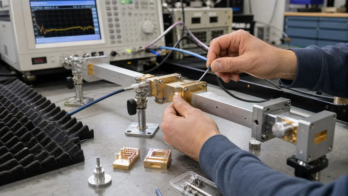
At short wavelengths, particles, burrs, face damage, cocking, pin wear, and unsupported weight can materially alter the path. Use inspection magnification appropriate to the interface, clean handling, dust caps, controlled fasteners, and rigid support that does not force alignment through the flange screws. Record the assembly order and orientation. Flexible waveguide or quasi-optical sections need their own alignment and repeatability method.
Put calibration planes on the mechanical drawing
Calibration of a frequency extender alone does not establish the DUT plane after added waveguide, adapters, probes, fixtures, or antennas. Mark calibration and measurement planes, error-box orientation, port numbering, standards, line lengths, environmental conditions, and software revision. For on-wafer work, include probe pitch, substrate, launch geometry, contact/planarity procedure, and wafer temperature.
TRL and multiline-TRL methods are powerful because transmission lines can establish propagation and reference impedance under defined assumptions, but line design, loss, dispersion, mode purity, reflect behaviour, and probe repeatability still contribute uncertainty. NIST’s terahertz mTRL work is direct evidence that on-wafer calibration artefacts and models are specialised engineering objects, not generic accessories. NIST’s 500–750 GHz waveguide calibration work likewise demonstrates the need for explicit calibration models and uncertainty at submillimetre wavelengths.
Verification should use a check artefact or path not merely recycled from the solve. Track complex S-parameters, power, or another relevant quantity over reassembly. De-embedding can shift the reported plane using characterized networks; it cannot repair an unknown flange state, mode conversion, drift, receiver compression, or a bad probe landing. Preserve raw and corrected data, calibration ID, de-embedding files, and port orientation.
Define uncertainty for the actual measurand
An output-power result may include power-reference calibration, detector linearity, mismatch, transition loss, frequency error, harmonic content, drift, repeat connection, and positioning. An S-parameter result additionally depends on calibration residuals, noise, dynamic range, reference impedance, flange/probe repeatability, and de-embedding. An antenna or material result includes free-space alignment and sample geometry. Use a separate model for each reported quantity.
Under the JCGM approach, list corrections and standard-uncertainty contributions with their distributions, sensitivity coefficients, correlations, and coverage. At mmWave/THz frequencies mismatch terms can be correlated and frequency dependent, so an unqualified root-sum-square of datasheet limits is not automatically valid. Report the result, plane, band, conditions, and uncertainty together.
| Selection problem | Primary design question | Evidence required before order |
|---|---|---|
| Harmonic generation | Can the source deliver the required drive and purity across the input band? | Drive sweep, multiplication factor, output band/power conditions, spur and filter plan |
| Receive extension | Can the chain detect the target without compression from leakage? | Gain/noise and maximum-input budgets, protection, LO/IF plan, calibration method |
| Passive routing | Are waveguide, flange, mode, loss and support compatible? | Dimensioned interface drawing, loss/return-loss data, assembly and repeatability method |
| On-wafer measurement | Can the reference plane be placed at the probe tips reproducibly? | Probe/substrate plan, mTRL or other method, planarity/contact verification, check artefact |
| Reconfigurable lab chain | Can operators rebuild it without changing the result beyond the budget? | Labels, keyed orientation, torque/support procedure, reassembly study and health limits |
Acceptance sequence for the assembled chain
Inspect and photograph interfaces, verify model/serial labels, and perform a dry mechanical fit without forcing alignment. Check bias polarity, current limits, control states, cooling, and interlocks before applying RF. Bring the chain up in a documented order with conservative drive and receiver protection. Confirm source and LO frequencies independently where practical.
Measure input match, output level or conversion response, unwanted products, and receiver margin across the required band and power states. Verify the calibration with an independent artefact, then disconnect/reconnect or reposition the defined interfaces for a repeatability study. Include thermal soak and cable/support movement if present in use. Run power-loss, overdrive, control-timeout, fan/cooling fault, and safe-shutdown tests for active hardware.
Store block-diagram revision, module serials, waveguide/flange IDs, orientation, fastener procedure, bias settings, source settings, instrument IDs, calibration and de-embedding IDs, raw data, environmental conditions, and acceptance decision. A screenshot without this chain of identity is weak evidence.
Failure modes that commonly escape a band-only review
- “THz” is used without a numerical frequency span or measurement goal.
- A multiplier’s output band overlaps the target, but the source cannot supply its required drive range.
- Ideal
20 log10(N)phase-noise translation is treated as complete output phase noise. - Typical module output is used as minimum DUT-plane power with no path-loss or mismatch budget.
- Two parts share a waveguide label but use incompatible flange or alignment-pin interfaces.
- Heavy modules are supported by mating flanges, producing connection-dependent stress.
- Calibration ends before an adapter or probe that dominates repeatability.
- De-embedding is used outside the model’s frequency, orientation, or physical revision.
- A receiver is protected in the nominal state but not during switching, startup, or fault.
- A harmonic peak is accepted as the desired signal without an unwanted-product check.
Illustrative worked example: a W-band x6 chain
This example is hypothetical system arithmetic, not an XGY acceptance result or guaranteed GT-W output. For a 92 GHz target using an ideal x6 multiplier, required source frequency is 92/6 = 15.333 GHz, within a nominal 12.5–18.33 GHz input band. Ideal phase-noise translation is 20 log10(6) = 15.56 dB; actual output adds multiplier residual noise and source/amplitude effects.
Suppose a planning value of 20 dBm exists at the module flange, then the chain has 1.8 dB transition loss, 0.7 dB waveguide loss, and a 10 dB protective attenuator. The arithmetic result is 20 - 1.8 - 0.7 - 10 = 7.5 dBm before mismatch and uncertainty. If a receiver maximum is 10 dBm, the nominal margin is only 2.5 dB and may be inadequate after output variation, attenuator tolerance, loss uncertainty, or a bypass fault. The correct action is a maximum-case protection budget and measurement, not assuming the nominal chain is safe.
Source-to-claim map
| Engineering statement in this article | Primary or official basis |
|---|---|
| Waveguide bands, dimensions, interfaces, performance, and interface uncertainty above 110 GHz require explicit definitions | IEEE 1785.1, 1785.2, and 1785.3 |
| Submillimetre-wave VNA calibration requires physical models and uncertainty evaluation | NIST 500–750 GHz calibration research |
| On-wafer THz calibration requires specialised probe/substrate line standards and reference planes | NIST terahertz mTRL research |
| Probing toward 1 THz creates specialised interconnect and calibration challenges | NIST submillimeter-wave probing programme |
| Frequency-band nomenclature has an official regulatory context but numerical spans remain essential | ITU Radio Regulations 2024 |
| An uncertainty result must follow a defined measurand and model | JCGM GUM and VIM |
| Competent laboratory operation includes method, equipment, and record controls | ISO/IEC 17025:2017 |
XGY product-data boundary
XGY product pages describe a portfolio envelope of 33 to 500 GHz with model-dependent WR-22 through WR-2.2 interfaces across active and passive components. The named GT-W-AM6-75110 is a specific x6 active multiplier with a published 12.5–18.33 GHz input and 75–110 GHz output; its page lists 100 mW as typical output, not an unconditional minimum across every frequency, drive, temperature, and interface state. Passive waveguide coverage and power handling are also component/configuration dependent.
These facts help build a shortlist but do not prove assembled-chain power, spectral purity, phase noise, noise figure, flange compatibility, calibration status, uncertainty, or safe receiver margin. Each quoted module must be matched by exact model, waveguide/flange drawing, operating conditions, bias/control data, and acceptance method. No portfolio-wide or customer-system performance is inferred here.
Product fit
XGY Tek options for mmWave and THz signal chains
The related active waveguide modules, W-band multiplier, and passive waveguide components are building-block candidates. Their suitability depends on a complete block diagram covering source drive, frequency plan, waveguide and flange interfaces, power and harmonics, calibration plane, mechanical mounting, bias or control, and acceptance evidence.
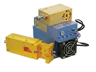
THz Modules
mmWave Active Waveguide Modules
XGY mmWave Active Waveguide Modules is a portfolio of standardized amplifier, multiplier, mixer, and converter building blocks covering 33 to 500 GHz for mmWave and sub-THz signal chains. The portfolio supports faster bring-up of Tx/Rx front-ends, extension chains, and test fixtures.
View product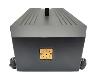
THz Modules
GT-W-AM6-75110 Full W-Band Active Multiplier
XGY GT-W-AM6-75110 is a full W-band active x6 frequency multiplier. It extends standard microwave sources (12.50 to 18.33 GHz) to a 75 to 110 GHz output frequency range, delivering typical output power of 100 mW for high-frequency test and characterization.
View product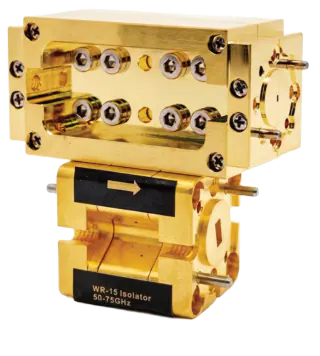
THz Modules
High Precision Passive Waveguide Components
XGY High Precision Passive Waveguide Components is a high-precision passive component portfolio for mmWave and THz signal chains. It includes fixed attenuators, directional and dual-directional couplers, waveguide filters, Faraday isolators, and waveguide-to-coaxial adapters.
View productFAQ
Frequently asked questions
What is the first artifact needed for a mmWave module quote?
The first artifact should be a signal-chain block diagram. It should show source frequency, multiplier or converter role, waveguide interface, flange type, expected power level, measurement instrument, calibration plane, and mechanical mounting. A bare frequency range leaves too many failure modes hidden.
Why does waveguide interface matter so much at W-band and above?
At W-band and above, small interface mismatches can create meaningful loss, reflections, alignment problems, and repeatability errors. Waveguide size, flange type, transition geometry, mounting orientation, and handling practice should be reviewed with the same seriousness as output power or frequency range.
When is an active module not enough to solve the measurement problem?
An active module is not enough when the source drive, harmonic filtering, receiver protection, calibration method, passive routing, mechanical support, or measurement instrument is mismatched. The module can meet its own datasheet and still fail the system if the surrounding chain is incomplete.
What should acceptance prove for a mmWave signal chain?
Acceptance should prove frequency plan, interface fit, output or received level, harmonic or unwanted-response control, calibration method, mounting repeatability, and any active bias or control behavior. For repeatable lab or production use, the evidence should include the configured signal path rather than only individual module datasheets.
Keep exploring
Related technical resources
Related articles
Technical Article
Phase-Stable RF Test Cable Buying Guide
How to evaluate phase-stable RF test cables for VNA measurement, production test, field use, and mmWave benches.
Read article
Technical Article
Choosing a PXIe VNA for Production RF Test
A buyer-focused guide to choosing PXIe vector network analyzers by frequency range, port count, dynamic range, slot width, and automation workflow.
Read article
Technical Article
RF Signal Generator Checklist for Receiver Test
How to select an RF signal generator for receiver sensitivity, radar, 5G, satellite, and automated RF test workflows.
Read article