
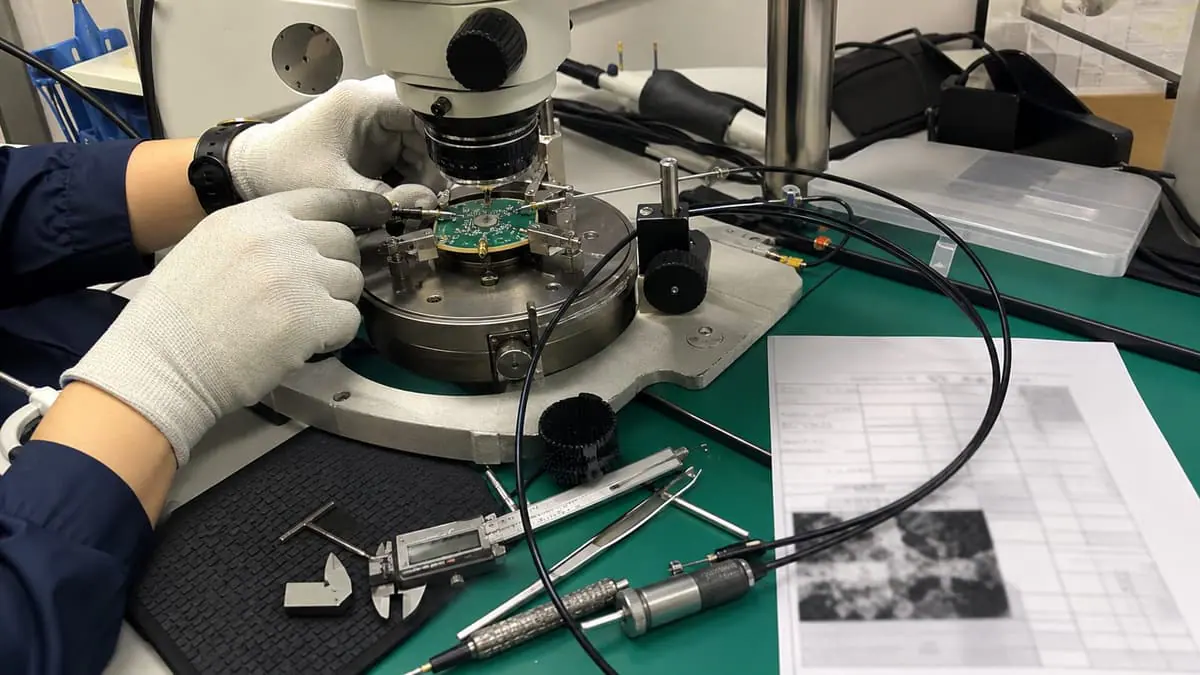
Use this semiconductor probe-station integration note before treating the station as a standalone purchase. It captures the inputs needed to quote the measurement chain: wafer size, pad pitch, probe count, RF or DC probe type, microscope requirements, chuck conditions, shielding, calibration substrates, and instrument interfaces.
The note is intended to help engineering and procurement teams compare a complete measurement chain rather than a standalone station. A probe station purchase can look simple at the catalog level, but stable wafer-level testing depends on the station, probes, microscope, chuck, cabling, shielding, calibration method, and connected instruments working together.
Workflows covered
The note is relevant to XMPS-208 manual probe station evaluations, RF probe selection, PXIe source-measure modules, VNA-based characterization workflows, leakage measurement, device characterization, RF S-parameter testing, packaged-device debug, and research benches where the DUT may change frequently.
For each workflow, the note asks whether the device is a full wafer, diced die, coupon, package, or custom substrate. It also asks for wafer size, die layout, pad pitch, pad metallurgy, number of probes, RF or DC probe type, frequency range, voltage/current limits, thermal needs, and whether the setup must be light-tight, shielded, or guarded for low-current measurements.
Instrument-chain inputs
The note encourages buyers to provide the connected instrument list early. Source measure units, VNAs, parameter analyzers, spectrum analyzers, and RF signal generators all create different cabling, grounding, calibration, and software requirements. For RF work, the note asks for calibration substrate, probe pitch, frequency range, cable routing, and calibration-plane expectations. For DC or leakage work, it asks for guarding, triax or coax cabling, shielded enclosure needs, and environmental constraints.
Microscope and operator workflow are also part of the scope. Buyers are asked to define magnification, illumination, camera needs, probe arm count, fine-positioning requirements, platen access, chuck movement, and whether several operators will share the station. These details affect repeatability and training.
Calibration, reporting, and acceptance
The integration note recommends defining calibration and data workflow before quotation. A useful wafer-level report can include wafer ID, die coordinates, probe configuration, instrument settings, operator, date/time, calibration status, and measured values. If the bench supports a quality or release process, buyers should also define calibration-document expectations for connected instruments.
Acceptance should include contact repeatability, probe landing procedure, calibration verification, instrument communication, data export, and at least one representative DUT workflow. If the station is delivered with a custom fixture or software sequence, those items should be included in factory acceptance and commissioning.
Review checkpoint
The integration note should be reviewed as a measurement-chain document. For an XMPS-208-style manual station, 8-inch wafer capability, up to 400 deg C temperature support, and 400X continuous zoom optics are meaningful only when matched to probe type, pad pitch, chuck conditions, calibration substrate, and the connected instruments. For SMU-based work, the reviewer should decide whether the XMU single/dual-channel high-voltage and low-current boundary or the multi-channel density boundary is the better fit.
Use the numbers as acceptance boundaries, not decorative specifications. A probe-station integration review can call out 200 mm wafer support, 4-inch / 6-inch / 8-inch chuck handling where relevant, 0.5 μm Z-axis adjustment precision, <2 μm probing resolution, +25°C to +400°C chuck operation, and ±1°C typical temperature accuracy. For RF probing, combine those station figures with probe constraints such as DC to 67 GHz coverage, 50 μm to 300 μm pitch options, <1.1 dB insertion loss to 40 GHz, and >14 dB return loss to 40 GHz.
The minimum review package should include a device geometry summary, a probe map, instrument list, calibration plan, environmental constraints, data fields, and acceptance sample. If RF probing is involved, add frequency range, probe pitch, cable routing, and calibration-plane definition. If leakage testing is involved, add guarding, shielding, light control, and contamination control.
Probe-station integration matrix
| Integration area | Evidence to provide | Rework trigger |
|---|---|---|
| Device geometry | Wafer or substrate size, die map, pad pitch, pad metallurgy, probe count, and keep-out zones | Station capability is discussed without a probe map or DUT drawing |
| RF measurement chain | Probe pitch, RF probe type, frequency range, cable path, calibration substrate, VNA port count, and calibration plane | S-parameter claims do not identify the probe, cable, calibration substrate, or instrument configuration |
| DC and leakage chain | SMU range, voltage compliance, current range, guarding, shielding, triax/coax choice, light control, and settling time | Low-current repeatability is blamed on the SMU before environment and cabling are controlled |
| Operator repeatability | Microscope setup, chuck movement, probe landing procedure, training notes, and sample workflow | Results depend on one experienced operator and cannot be repeated by the receiving team |
| Data and acceptance | Wafer ID, die coordinate, probe configuration, instrument settings, calibration status, operator, date/time, and report export | The station is delivered as hardware but not as a documented measurement workflow |
Engineering FAQ
What makes probe station selection different from ordinary instrument selection?
The probe station defines the physical measurement plane. Pad pitch, probe landing repeatability, chuck temperature, microscope access, shielding, cable routing, and calibration substrate choice can change the measurement as much as the SMU or VNA specification.
What should be defined for RF wafer probing?
Define frequency range, probe pitch, RF probe type, cable path, calibration substrate, calibration plane, VNA port count, connector wear strategy, and whether measurements require S-parameters, gain, return loss, isolation, or noise-related data. The probe and calibration plan should be scoped with the VNA, not after it.
What should be defined for low-current or leakage probing?
Define guarding, shielding, triax or coax cabling, light control, contamination control, settling time, current range, voltage compliance, and allowed probe contact force. Low-current repeatability often fails through environment and cabling before it fails through the SMU.
What proves the delivered station is ready to use?
Acceptance should include a representative DUT workflow, contact repeatability check, calibration verification, instrument communication, data export, operator handover, and a report sample that records wafer ID, die coordinates, probe configuration, instrument settings, and calibration status.
Using the note
Before contacting XGY Tek, buyers can use the note to gather wafer or substrate dimensions, pad pitch, expected probe count, RF/DC requirements, voltage/current or frequency range, thermal conditions, shielding needs, calibration substrates, instrument interfaces, and report format.
That package gives XGY Tek a practical basis for matching the probe station, probes, SMUs, VNAs, shielding, and software workflow to the real semiconductor test requirement.