
X-Ray Inspection Systems
AXI-300 High-Speed In-Line 3D X-Ray Inspection System
Inline 3D X-Ray Inspection for Electronic Assemblies
AXI-300 uses tomographic fusion and tomosynthesis for layered inspection of electronic assemblies and semiconductor packaging. It supports welding-surface inspection and void-size / void-rate analysis for BGA, QFN/THT, stacked-chip, IGBT and SiC applications.
Get a Quote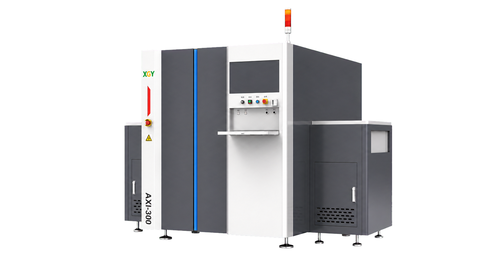
- Inspection envelope
- 300(X) mm x 300(Y) mm maximum inspection size
- Minimum detectable defect size
- ≤ 5 µm
- X-ray leakage dose
- <0.5 uSv/h
- X-ray source
- 110 kV / 130 kV / 150 kV maximum voltage
Overview
AXI-300 uses tomographic fusion and tomosynthesis for layered inspection of electronic assemblies and semiconductor packaging. It supports welding-surface inspection and void-size / void-rate analysis for BGA, QFN/THT, stacked-chip, IGBT and SiC applications.
Product & Measurement Gallery
AXI-300 Inspection Software Interface
AXI-300 Inline System and Transfer-Track Layout
The equipment configuration image shows the inline loading and unloading relationship used for lead-room connection.
Fly-Shooting Synchronized Motion Layout
The fly-shooting layout shows the synchronous X-ray source and detector motion used to improve acquisition efficiency.
3D X-Ray Tomosynthesis Working-Principle Diagram
The principle diagram places the tested object between the X-ray source and detector, with the detector and source moving around their revolution planes. This visual anchors the later inspection examples by explaining how the system acquires layered X-ray information.
Layer-Separated Void-Analysis Result
Traditional 2D Projection View
The 2D projection provides the baseline for comparing conventional projection output with separated 3D layer views.
Chip-Layer Reconstructed Inspection View
The chip-layer 3D view corresponds to the inspection requirement for locating voids in the chip layer.
DBC-Layer Reconstructed Inspection View
The DBC-layer 3D view is paired with the chip-layer example to show depth-specific defect separation.
IGBT Inspection Result
The IGBT result and layered welding samples show how inspection output translates layer information into visible defect regions.
Layered Welding Inspection Result
SiC High-Resolution Inspection Result
The high-resolution and molybdenum result samples extend the inspection narrative from SiC and advanced modules to dense difficult-metal structures.
Molybdenum Inspection Result
Traditional 2D View for Special-Material Comparison
Rework-Station Inspection Result
Three-Section Lead-Shielded Transfer-Rail Layout
The rail layout view supports the inline automation story: loading, inspection, and output handling are organized around the equipment body.
IGBT Weld Sample for X-Ray Inspection
Application images show typical use settings; they do not indicate measured performance.
Pin-Fin Module Sample for X-Ray Inspection
Application images show typical use settings; they do not indicate measured performance.
SiC Module Sample for X-Ray Inspection
Application images show typical use settings; they do not indicate measured performance.
Advanced-Package Sample for X-Ray Inspection
Application images show typical use settings; they do not indicate measured performance.
Difficult-Metal Sample for X-Ray Inspection
Application images show typical use settings; they do not indicate measured performance.
Additional product details
The integrated configuration combines high-speed acquisition, lead-proof transfer rails, software customization, rework support, and inline factory connectivity under the AXI-300 model.
Key Capabilities & Applications
Layered 2D/3D analysis
Tomosynthesis separates internal layers for welding-surface and void inspection. The listed minimum detectable defect size is ≤5 µm.
Configurable imaging platform
An enclosed 110 / 130 / 150 kV source configuration works with a 16-bit flat-panel detector, 3072 × 3072 pixels and a 304 × 304 mm effective area.
Inline factory integration
Connections to MES, ERP and WMS support factory integration. Inline control and barcode readers are configurable.
Common applications
- BGA inspection
- QFN and THT inspection
- Stacked-chip inspection
- IGBT and SiC power modules
- Advanced packaging
- Dense materials and high-density PCBs
Applications and test requirements
BGA inspection
Layered X-ray inspection for hidden BGA solder joints and void analysis.
QFN and THT inspection
2D and 3D inspection of QFN and through-hole assembly structures.
Stacked-chip inspection
Tomosynthesis separates overlapping internal layers in stacked-chip assemblies.
IGBT and SiC power modules
Layer-specific inspection supports IGBT, SiC, DBC, chip, and welding-surface analysis.
Advanced packaging
Non-destructive inspection for advanced semiconductor-package structures and internal defects.
Dense materials and high-density PCBs
X-ray inspection supports difficult-metal samples and high-density PCB back-drilling workflows.
Technical Specifications
| Parameter | Specification |
|---|---|
| X-ray source | Enclosed; 110 kV / 130 kV / 150 kV maximum voltage |
| Source current and power | 300 µA / 300 µA / 500 µA; 30 W / 39 W / 75 W |
| Detector | High-resolution 16-bit FPD; 304 mm × 304 mm effective area |
| Detector matrix | 3072 × 3072 pixels; 99 µm pixel size |
| Inspection envelope | 350(X) mm x 350(Y) mm maximum load; 300(X) mm x 300(Y) mm maximum inspection size |
| Minimum detectable defect size | ≤ 5 µm |
| Maximum sample weight | 8 kg |
| Power requirement | 6.5 kW |
View all 13 specifications
| Parameter | Specification |
|---|---|
| Machine envelope | 1624(L) x 2283(W) x 2226(H) mm excluding connecting rail; approximately 4500 kg |
| Power supply | 220 to 230 V / 50 Hz |
| X-ray leakage dose | <0.5 uSv/h |
| Factory connectivity | Supports connection with MES, ERP, WMS, and other inline management systems |
| Inspection tilt angle | ≥20° |
Detailed performance and interface tables (1)
| Parameter | Value |
|---|---|
| X-Ray Source | |
| Type | Enclosed |
| Maximum voltage | 110 kV / 130 kV / 150 kV |
| Maximum current | 300 µA / 300 µA / 500 µA |
| Maximum power | 30 W / 39 W / 75 W |
| Detector | |
| Type | High-resolution FPD |
| AD conversion bits | 16 bit |
| Effective detection area | 304 mm × 304 mm |
| Pixel matrix | 3072 × 3072 pixels |
| Pixel size | 99 µm |
| Computer | |
| Monitor | 24-inch HD monitor |
| Operating system | Windows 10 |
| Inspection Capability | |
| Maximum load size | 350(X) mm x 350(Y) mm |
| Maximum inspection size | 300(X) mm x 300(Y) mm |
| Maximum sample weight | 8 kg |
| Software System | |
| Software introduction | XGY In-Line 3D X-ray Tomosynthesis Technology Software V1.0 |
| Inspection functions | 2D and 3D scanning inspection; welding surface layered inspection, void size and void-rate analysis |
| Overall Machine Parameters | |
| Equipment body size | 1624(L) x 2283(W) x 2226(H) mm, excluding connecting rail |
| Weight | Approximately 4500 kg |
| Power supply | 220 to 230 V / 50 Hz |
| Power supply power | 6.5 kW |
| Safety control | Emergency Stop Switch / EMO Switch |
| Options and Integration | |
| Customizable options | Maintenance workstations, offline programming, barcode readers, lead-room connecting tracks, and integrated inline control systems |
| Factory connectivity | Supports connection with MES, ERP, WMS, and other inline management systems |
- Specifications should be confirmed against the latest order configuration before purchase.
Specifications are subject to change without notice.
Models, Configuration & Compatibility
AXI-300
Control interfaces and software
XGY In-Line 3D X-ray Tomosynthesis Technology Software V1.0 supports 2D/3D inspection, layered welding-surface inspection, and void-size / void-rate analysis. Factory integration supports connections with MES, ERP, WMS and other inline management systems; inline control and barcode readers are configurable.
MES / ERP / WMS · 2D / 3D inspection
Order codes and configuration are confirmed in the quotation.
Technical Resources
Selection guidance
Format: Inline 3D X-ray inspection system
Coverage: 300 mm × 300 mm inspection area; 8 kg maximum sample weight; 3D tomosynthesis
Best for: BGA, QFN/THT, IGBT, SiC, advanced packaging, difficult-metal, and high-density PCB inspection workflows.
View the X-Ray Inspection Systems categorySend the operating envelope, configuration and acceptance evidence you need; the quotation confirms model, options and delivery documentation.