
Products
X-Ray Inspection Systems
Inline 3D X-Ray Inspection for Internal Defect Analysis
XGY X-ray inspection systems are designed for production and engineering workflows where internal solder joints, power-module welding layers, stacked packages, or dense materials require non-destructive inspection. The parameter that binds first is what has to be resolved through the assembly rather than how fast the line runs: a conventional 2D projection sums every layer along the beam path, so a void under a die and a void under the DBC substrate arrive as one shadow and cannot be assigned to a layer.
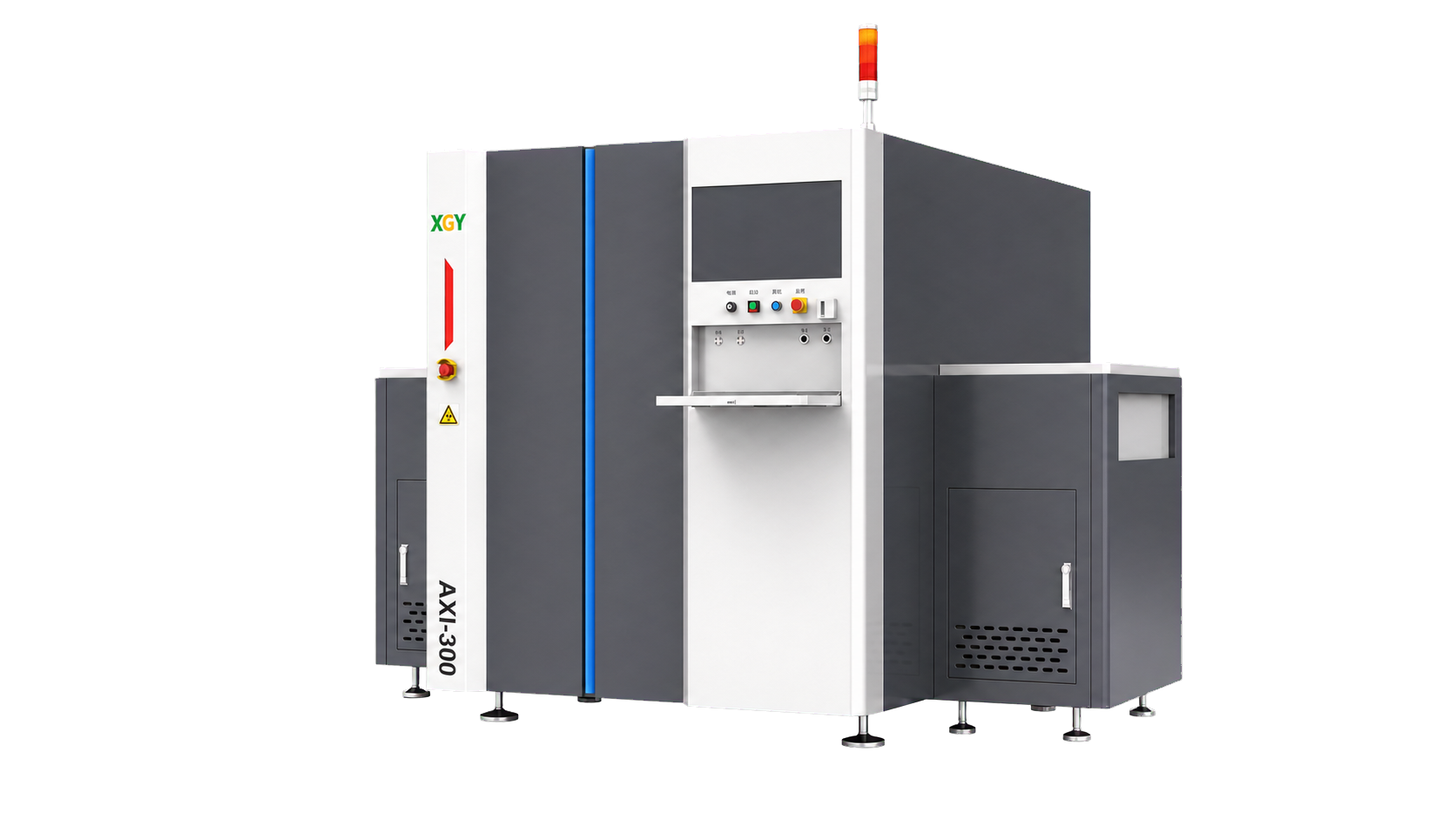
The AXI-300 answers that with tomosynthesis reconstruction, combining 2D and 3D scanning, layer separation, void-size and void-rate analysis, inline transfer rails, and factory-system connectivity in one platform. Its published envelope sets the second constraint: a 300(X) mm x 300(Y) mm maximum inspection size inside a 350(X) mm x 350(Y) mm load, 8 kg maximum sample weight, a 16-bit flat-panel detector of 304 mm x 304 mm at 99 um pixel size, 110 kV, 130 kV or 150 kV source options, and a minimum detectable defect size of 5 um or smaller.
An inspection result is only credible when the record carries the source voltage and current, the magnification and tilt angle, the reconstructed layer, the void criterion applied, the software version, and the sample identifier - a void rate quoted without the layer it was measured on is not a comparable number.
The source, detector, inspection envelope, rail configuration, software options, line-integration interfaces, and the site radiation-safety approvals should be confirmed against the intended order configuration before a quotation is issued.
Selection path
X-Ray inspection system selection
Compare the stated inspection envelope, sample-weight limit, scanning mode, and integration requirements before selecting a configuration.
- AXI-300Inline 3D X-ray inspection system
- Coverage
- 300 mm × 300 mm inspection area; 8 kg maximum sample weight; 3D tomosynthesis
- Best fit
- BGA, QFN/THT, IGBT, SiC, advanced packaging, difficult-metal, and high-density PCB inspection workflows.